1. Crystal Structure and Polytypism of Silicon Carbide
1.1 Cubic and Hexagonal Polytypes: From 3C to 6H and Past
(Silicon Carbide Ceramics)
Silicon carbide (SiC) is a covalently bonded ceramic composed of silicon and carbon atoms organized in a tetrahedral sychronisation, forming one of the most complex systems of polytypism in materials science.
Unlike many porcelains with a solitary steady crystal framework, SiC exists in over 250 known polytypes– distinctive piling series of close-packed Si-C bilayers along the c-axis– ranging from cubic 3C-SiC (likewise known as β-SiC) to hexagonal 6H-SiC and rhombohedral 15R-SiC.
One of the most usual polytypes used in design applications are 3C (cubic), 4H, and 6H (both hexagonal), each displaying somewhat different digital band structures and thermal conductivities.
3C-SiC, with its zinc blende structure, has the narrowest bandgap (~ 2.3 eV) and is normally expanded on silicon substratums for semiconductor tools, while 4H-SiC offers remarkable electron movement and is favored for high-power electronic devices.
The strong covalent bonding and directional nature of the Si– C bond confer outstanding hardness, thermal stability, and resistance to slip and chemical assault, making SiC ideal for extreme environment applications.
1.2 Defects, Doping, and Electronic Residence
Regardless of its architectural complexity, SiC can be doped to attain both n-type and p-type conductivity, allowing its usage in semiconductor tools.
Nitrogen and phosphorus act as donor impurities, introducing electrons into the transmission band, while aluminum and boron work as acceptors, creating openings in the valence band.
However, p-type doping effectiveness is restricted by high activation powers, especially in 4H-SiC, which presents difficulties for bipolar device style.
Native issues such as screw misplacements, micropipes, and piling mistakes can weaken device performance by acting as recombination centers or leakage paths, requiring top quality single-crystal growth for electronic applications.
The large bandgap (2.3– 3.3 eV depending on polytype), high breakdown electrical area (~ 3 MV/cm), and exceptional thermal conductivity (~ 3– 4 W/m · K for 4H-SiC) make SiC far above silicon in high-temperature, high-voltage, and high-frequency power electronics.
2. Processing and Microstructural Design
( Silicon Carbide Ceramics)
2.1 Sintering and Densification Methods
Silicon carbide is inherently difficult to densify as a result of its solid covalent bonding and low self-diffusion coefficients, requiring advanced processing techniques to accomplish full thickness without ingredients or with marginal sintering aids.
Pressureless sintering of submicron SiC powders is possible with the enhancement of boron and carbon, which promote densification by removing oxide layers and improving solid-state diffusion.
Hot pushing applies uniaxial stress throughout home heating, enabling full densification at lower temperature levels (~ 1800– 2000 ° C )and generating fine-grained, high-strength components appropriate for reducing devices and wear parts.
For large or intricate forms, reaction bonding is utilized, where porous carbon preforms are infiltrated with molten silicon at ~ 1600 ° C, developing β-SiC in situ with minimal shrinkage.
However, residual complimentary silicon (~ 5– 10%) stays in the microstructure, restricting high-temperature performance and oxidation resistance above 1300 ° C.
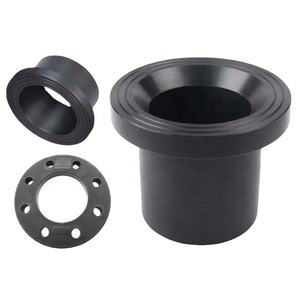
2.2 Additive Manufacturing and Near-Net-Shape Manufacture
Current breakthroughs in additive production (AM), specifically binder jetting and stereolithography utilizing SiC powders or preceramic polymers, allow the manufacture of complicated geometries previously unattainable with traditional approaches.
In polymer-derived ceramic (PDC) paths, fluid SiC forerunners are shaped using 3D printing and after that pyrolyzed at heats to yield amorphous or nanocrystalline SiC, usually requiring additional densification.
These techniques decrease machining prices and product waste, making SiC extra obtainable for aerospace, nuclear, and heat exchanger applications where intricate designs improve performance.
Post-processing actions such as chemical vapor seepage (CVI) or fluid silicon infiltration (LSI) are in some cases used to enhance density and mechanical integrity.
3. Mechanical, Thermal, and Environmental Efficiency
3.1 Strength, Solidity, and Put On Resistance
Silicon carbide places amongst the hardest well-known materials, with a Mohs solidity of ~ 9.5 and Vickers hardness surpassing 25 Grade point average, making it extremely immune to abrasion, erosion, and damaging.
Its flexural stamina commonly varies from 300 to 600 MPa, relying on handling method and grain size, and it maintains strength at temperature levels approximately 1400 ° C in inert ambiences.
Crack strength, while modest (~ 3– 4 MPa · m 1ST/ ²), suffices for many architectural applications, especially when integrated with fiber support in ceramic matrix composites (CMCs).
SiC-based CMCs are made use of in wind turbine blades, combustor liners, and brake systems, where they supply weight financial savings, gas performance, and expanded life span over metal counterparts.
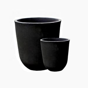
Its excellent wear resistance makes SiC perfect for seals, bearings, pump components, and ballistic shield, where durability under extreme mechanical loading is essential.
3.2 Thermal Conductivity and Oxidation Stability
One of SiC’s most useful properties is its high thermal conductivity– up to 490 W/m · K for single-crystal 4H-SiC and ~ 30– 120 W/m · K for polycrystalline types– exceeding that of lots of metals and enabling efficient warmth dissipation.
This residential or commercial property is vital in power electronics, where SiC gadgets create less waste warmth and can run at greater power thickness than silicon-based devices.
At elevated temperatures in oxidizing environments, SiC forms a safety silica (SiO TWO) layer that reduces further oxidation, supplying great environmental resilience as much as ~ 1600 ° C.
Nevertheless, in water vapor-rich atmospheres, this layer can volatilize as Si(OH)₄, bring about sped up degradation– a vital difficulty in gas generator applications.
4. Advanced Applications in Power, Electronics, and Aerospace
4.1 Power Electronic Devices and Semiconductor Gadgets
Silicon carbide has changed power electronics by enabling gadgets such as Schottky diodes, MOSFETs, and JFETs that run at greater voltages, frequencies, and temperature levels than silicon equivalents.
These devices reduce energy losses in electrical lorries, renewable resource inverters, and industrial motor drives, contributing to global power effectiveness enhancements.
The capacity to operate at junction temperatures over 200 ° C permits simplified air conditioning systems and boosted system integrity.
In addition, SiC wafers are used as substratums for gallium nitride (GaN) epitaxy in high-electron-mobility transistors (HEMTs), integrating the benefits of both wide-bandgap semiconductors.
4.2 Nuclear, Aerospace, and Optical Systems
In nuclear reactors, SiC is a crucial component of accident-tolerant fuel cladding, where its low neutron absorption cross-section, radiation resistance, and high-temperature toughness boost security and efficiency.
In aerospace, SiC fiber-reinforced compounds are made use of in jet engines and hypersonic vehicles for their light-weight and thermal security.
Furthermore, ultra-smooth SiC mirrors are employed in space telescopes because of their high stiffness-to-density ratio, thermal security, and polishability to sub-nanometer roughness.
In recap, silicon carbide ceramics represent a keystone of contemporary sophisticated materials, combining remarkable mechanical, thermal, and digital homes.
Through accurate control of polytype, microstructure, and processing, SiC continues to make it possible for technical innovations in energy, transportation, and severe atmosphere engineering.
5. Vendor
TRUNNANO is a supplier of Spherical Tungsten Powder with over 12 years of experience in nano-building energy conservation and nanotechnology development. It accepts payment via Credit Card, T/T, West Union and Paypal. Trunnano will ship the goods to customers overseas through FedEx, DHL, by air, or by sea. If you want to know more about Spherical Tungsten Powder, please feel free to contact us and send an inquiry(sales5@nanotrun.com).
Tags: silicon carbide ceramic,silicon carbide ceramic products, industry ceramic
All articles and pictures are from the Internet. If there are any copyright issues, please contact us in time to delete.
Inquiry us